Company details for:
SiSTEM Technology Limited
Quick Links:
Products / Services
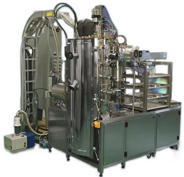
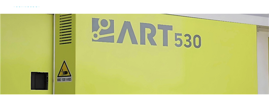
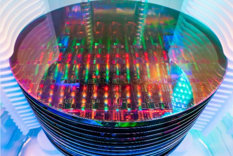
Thin Film Deposition Products
There are several thin film deposition techniques, each with its own specialised equipment. Some of the most widely used methods include:
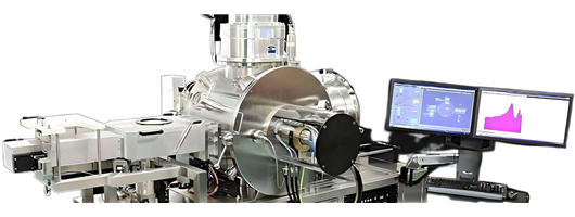
Physical Vapour Deposition (PVD): PVD equipment, such as sputtering and evaporation systems, utilizes physical processes to deposit thin films by condensing vaporized materials onto the substrate.
Chemical Vapour Deposition (CVD): CVD equipment deposits thin films through chemical reactions involving gas-phase precursors. Common CVD techniques include plasma-enhanced CVD (PECVD), low-pressure CVD (LPCVD), and atomic layer deposition (ALD).
Electrochemical Deposition: This technique uses electrochemical processes to deposit thin films, often employed in the fabrication of semiconductor devices and MEMS.
Atomic Layer Deposition (ALD): ALD equipment enables highly precise and conformal deposition by using alternating self-limiting chemical reactions to build layers one atom at a time.
Each deposition technique offers unique advantages in terms of film quality, conformality, and process control, making them suitable for various applications within the semiconductor industry. By employing advanced thin film deposition equipment, manufacturers can continue to innovate and drive the development of increasingly powerful electronic devices.
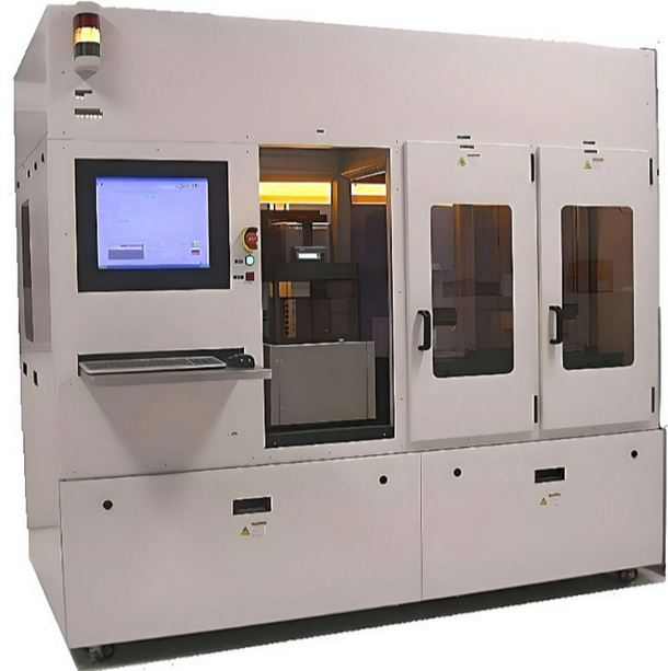
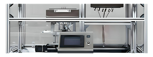
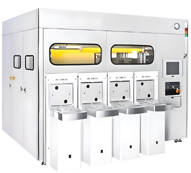
Reticle & Wafer Handling & Automation Products
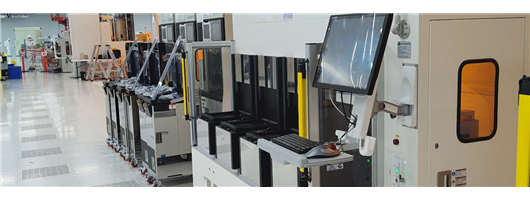
The semiconductor manufacturing process involves numerous intricate steps, such as wafer & reticle handling, photolithography, etching, deposition, and inspection, which require precise control and coordination. Handling and automation equipment, including robotic arms, automated material handling systems (AMHS), wafer sorters, and automated test equipment (ATE), enable seamless integration of these processes and improve overall productivity.
Automation equipment is designed to operate within cleanroom environments, adhering to strict cleanliness standards to prevent contamination, which can negatively impact the performance and yield of semiconductor devices. These systems also enhance safety by reducing human contact with hazardous materials, high-voltage equipment, and other potential risks associated with semiconductor manufacturing.
Investment in handling and automation equipment is essential for the semiconductor industry to meet the growing demand for high-performance devices, reduce production costs, and maintain a competitive edge in an ever-evolving technological landscape.
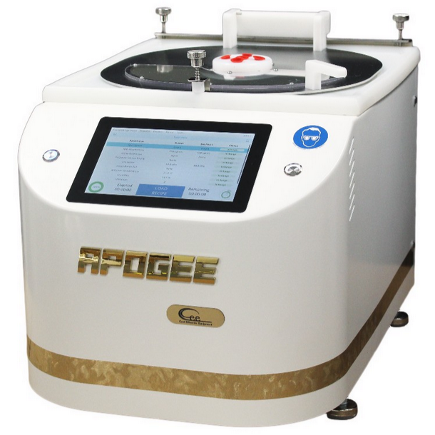
Wafer Processing Equipment
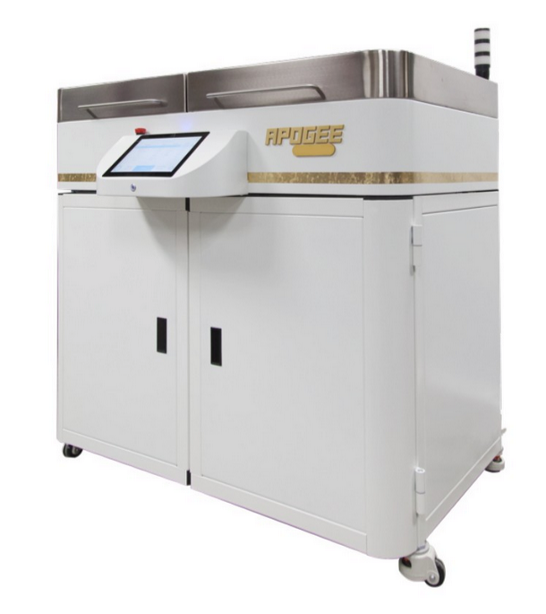
Originally known as Brewer Science, who evolved into a materials company, Cost Effect Equipment Apogee spin coaters, spin developers and spin cleaners as well as hot plates and chill plates are trusted by experts worldwide for their exceptional performance in applications such as photoresist and anti-reflective coatings, e-beam resists, sol-gels, packaging adhesives, dielectrics, and more. With decades of experience in coating and baking semiconductor wafers, MEMS devices, flat panel displays, photomasks, and bio-medical devices, our CEE products offer unparalleled flexibility and reliability.
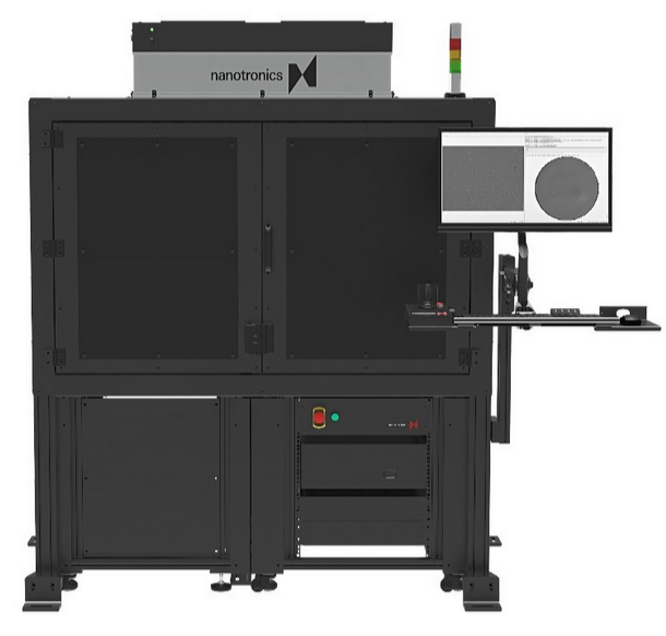
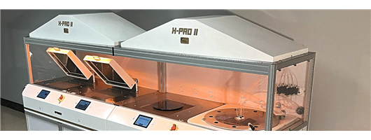
Optical Defect Inspection
Nanotronics, a leading provider of optical defect inspection solutions, offers a range of advanced products that combine high-resolution imaging, artificial intelligence, and automation to deliver accurate, reliable, and efficient inspection capabilities. Their systems are designed to detect defects, measure dimensions, and analyse surface characteristics with exceptional precision, enabling manufacturers to identify and address issues early in the production process.
One of the key strengths of Nanotronics’ optical defect inspection products is the integration of machine learning algorithms, which enables the systems to adapt and improve their performance over time, reducing false alarms and increasing defect detection accuracy. These systems also offer high-speed inspection capabilities, minimising inspection times and enabling real-time process control.
By leveraging the cutting-edge technology in Nanotronics’ optical defect inspection products, manufacturers can enhance product quality, reduce scrap rates, and optimise overall production efficiency. This, in turn, contributes to increased competitiveness and profitability in today’s demanding market landscape.
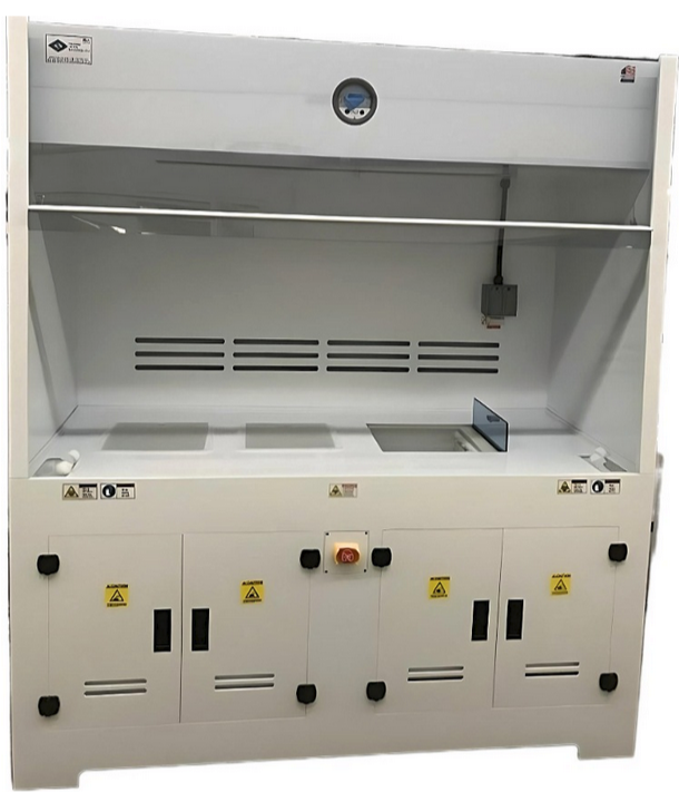
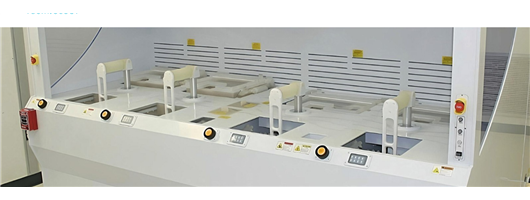
Wet Processing Products
Key wet processing products and equipment used in the semiconductor industry include wet benches, chemical baths, spin processors, and rinse systems. Wet benches provide a dedicated work area for manual or automated wet processing, ensuring a clean and controlled environment. Chemical baths are used for immersion processes, such as etching or cleaning, where the substrate is submerged in a specific chemical solution.
Spin processors are employed for spin coating and developing photoresist layers, offering precise control over film thickness and uniformity. Rinse systems, on the other hand, play a critical role in removing residual chemicals and particles from substrates after processing, ensuring the cleanliness and quality of the wafer surface.
Wet processing products and equipment are integral to the semiconductor industry, as they enable the execution of critical manufacturing steps that impact device performance and yield. By utilising advanced wet processing solutions, semiconductor manufacturers can continue to drive innovation and produce increasingly powerful electronic devices for the global market.
Temporary Wafer Bond & Debond Tools
Temporary wafer bonding is vital for the production of 3D integrated circuits (ICs), power devices, and Fan-Out Wafer Level Packaging (FoWLP) wafers, as well as in managing delicate substrates such as compound semiconductors.
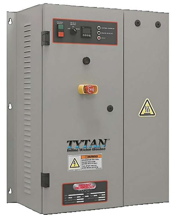
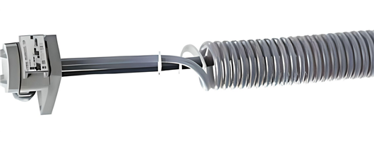
Water & Chemical Heaters
Several types of heaters are available for heating chemicals, including hot plates, heating mantles, oil baths, water baths, and sand baths. Each type has its advantages and application areas, depending on factors such as the required temperature range, chemical compatibility, and the nature of the container holding the chemicals.
Safety features, such as over-temperature protection and chemical-resistant materials, are often incorporated in these heaters to prevent accidents and damage. Proper use of chemical heaters is crucial, as uncontrolled heating can lead to hazardous situations, including chemical spills, fires, or explosions. In many cases, temperature controllers and monitors are used in conjunction with these heaters to ensure the desired temperature is maintained throughout the process.
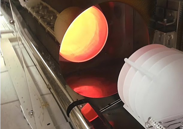
Thermal Processing Products
Process Technology’s thermal processing products include high-performance inline and immersion heaters, temperature control units, and heat exchangers. These products are designed to provide precise and uniform temperature control, ensuring consistent process conditions and enabling the production of high-quality components and devices.
One of the key strengths of Process Technology’s thermal processing products is their robust construction, which ensures reliability and durability under challenging operating conditions. These products are engineered with advanced materials and technologies, such as fluoropolymer and high-purity quartz, to provide excellent chemical resistance and superior thermal performance.
By offering versatile, reliable, and efficient thermal processing solutions, Process Technology supports manufacturers in achieving their process goals and maintaining a competitive edge in the market. As the demand for advanced electronic devices continues to grow, Process Technology’s commitment to innovation and quality ensures that their thermal processing products remain at the forefront of industry requirements, enabling manufacturers to produce cutting-edge products for the global market.
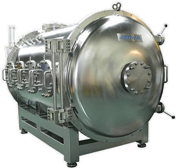
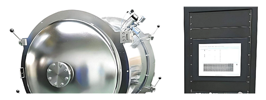
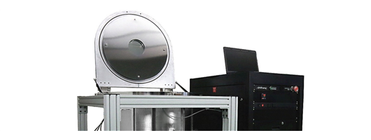
Thermal Vacuum (TVAC) Products
Intlvac’s thermal vacuum products include advanced thermal vacuum chambers, custom-engineered vacuum systems, and related accessories. These systems are designed to simulate extreme environmental conditions, such as the vacuum and temperature variations experienced in space, enabling manufacturers and researchers to test and qualify components and devices under realistic operating conditions.
One of the key strengths of Intlvac’s thermal vacuum products is their precision engineering, which ensures high-performance vacuum and temperature control. These products incorporate cutting-edge materials and technologies, such as cryogenic and resistive heating systems, to provide accurate and uniform temperature profiles and vacuum levels.
By offering versatile and reliable thermal vacuum solutions, Intlvac supports manufacturers and researchers in achieving their process and testing goals, contributing to advancements in various fields. Intlvac’s commitment to innovation and quality ensures that their thermal vacuum products remain at the forefront of industry requirements, enabling the development and qualification of high-performance components and devices for challenging applications.
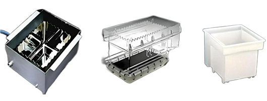
Megasonics Products
ProSys, a leading provider of megasonic cleaning solutions, offers a range of high-performance products that deliver superior cleaning results while minimising damage to sensitive components. ProSys’ megasonic cleaning systems use powerful transducers to generate megasonic waves, which create microscopic cavitation bubbles that implode upon contact with the surface, effectively removing contaminants such as particles, organic residues, and thin films.
One of the key advantages of ProSys’ megasonic cleaning products is their ability to provide uniform and controlled energy distribution across the cleaning surface, ensuring consistent cleaning performance and reduced risk of component damage. These systems can be easily integrated into various processes and are compatible with a wide range of chemistries, enabling versatile and efficient cleaning solutions for diverse applications.
By leveraging the capabilities of megasonics, ProSys enables manufacturers to achieve high levels of cleanliness and process control, contributing to improved product quality and yield in demanding industries.
Degassing Systems
Trapped gases within components can cause a range of issues, including voids, bubbles, and structural defects, which can lead to reduced mechanical strength, electrical conductivity, or thermal stability. Degassing systems help mitigate these issues by eliminating gases before or during the manufacturing process.
Several techniques are employed in degassing systems for components, including vacuum degassing, thermal degassing, and centrifugal degassing. Vacuum degassing involves placing the components in a vacuum chamber, reducing the pressure to facilitate gas release. Thermal degassing uses heat to increase the gas solubility and vaporize trapped substances. Centrifugal degassing applies a high-speed spinning force to separate gases from denser materials.
These systems are widely used in processes such as resin casting, potting and encapsulation, adhesive bonding, and soldering. Proper degassing ensures the reliability, durability, and overall quality of components, ultimately contributing to the performance and lifespan of the final product.
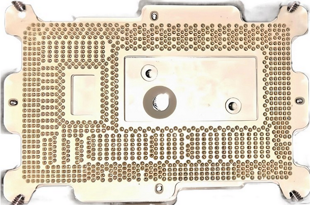
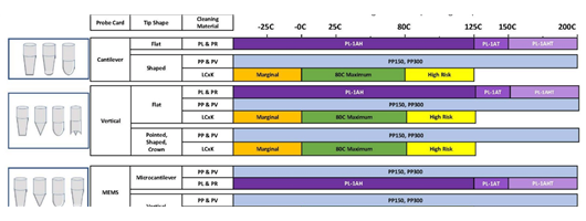
Probe, Test & Burn-In Products
Probe products, such as wafer probe stations and probe cards, are used to test semiconductor wafers before they are diced and packaged, ensuring that individual die meet the required electrical and functional specifications. This step is critical for identifying and isolating defective die, preventing their incorporation into finished products.
Test products, which include automated test equipment (ATE), are utilised to test the functionality and performance of packaged semiconductor devices. ATE systems can perform a variety of tests, such as power-up, digital, and analog testing, to verify that devices meet design and quality standards.
Burn-in products, like burn-in ovens and test sockets, subject semiconductor devices to accelerated aging conditions, such as elevated temperatures and electrical stress, to identify potential reliability issues and screen out early-life failures. This process helps to ensure the long-term stability and performance of electronic components.
By employing probe, test, and burn-in products, manufacturers can enhance product quality, reduce costs associated with defects, and ultimately improve customer satisfaction.
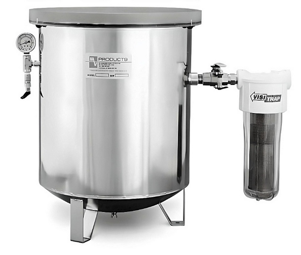
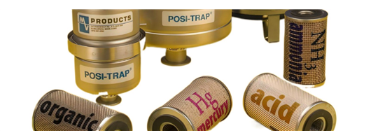
Vacuum Chambers, Traps & Consumables
Some key vacuum products and equipment used in the semiconductor industry include thermal vacuum chambers (TVAC), vacuum pumps, valves, and vacuum traps. Vacuum pumps generate the required vacuum levels by removing gases from the processing chamber, while vacuum chambers provide an enclosed space for the execution of various processes, such as thin film deposition, etching, degassing, and testing under certain conditions.
Vacuum traps, on the other hand, are essential components that protect vacuum pumps and systems from contaminants, such as particulates and reactive gases. These traps help maintain the cleanliness and integrity of the vacuum environment, which is crucial for achieving high yields and product quality.
Vacuum consumables, products, and equipment, including vacuum traps, are integral to the semiconductor industry, as they provide the necessary conditions for advanced manufacturing processes. By employing reliable and efficient vacuum solutions, semiconductor manufacturers can continue to innovate and produce increasingly powerful electronic devices for the global market.
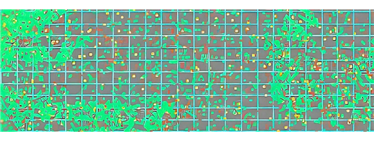
Chuck Cleaning Wafers
Particle Removal: Semiconductor manufacturing processes are highly sensitive to contamination. Chuck cleaning wafers help remove particles, residues, and contaminants that can accumulate on the chuck surface over time. By effectively cleaning the chuck, these wafers help minimise the risk of particle transfer onto the wafers being processed, ensuring higher product quality and yield.
Improved Yield: Contamination on the chuck surface can lead to defects during the manufacturing process. Chuck cleaning wafers help maintain a clean and smooth chuck surface, reducing the likelihood of defects caused by particle adhesion or uneven contact between the wafer and the chuck. This, in turn, improves the overall yield of the semiconductor fabrication process.
... And more.
Semiconductor Manufacturing Spares & Consumables

Installation

Warranty Support
Preventatative Maintenance
About us
Welcome to SiSTEM Technology, your reliable sales and distribution partner specialising in the semiconductor, nanotechnology, biotechnology, and precision R&D and manufacturing sectors.
Our steadfast dedication is centred around deeply understanding the distinct challenges you face, enabling us to provide transparent and effective solutions that are not only honest but also mindful of your budget constraints.
When you choose to partner with us, you benefit from a dedicated team that consistently goes above and beyond to ensure your success. We prioritise building enduring relationships based on trust and mutual prosperity, aiming to cultivate a partnership that lasts well into the future. At every step, our goal is to deliver tailored solutions that meet your needs and contribute to the sustained growth and achievement of your objectives.
Our Solutions Include:
Thin Film
Thin film deposition equipment, utilised for physical vapor deposition (PVD) and chemical vapor deposition (CVD), is specialised and essential for producing thin films crucial to various electronic devices like integrated circuits, solar cells, and displays.
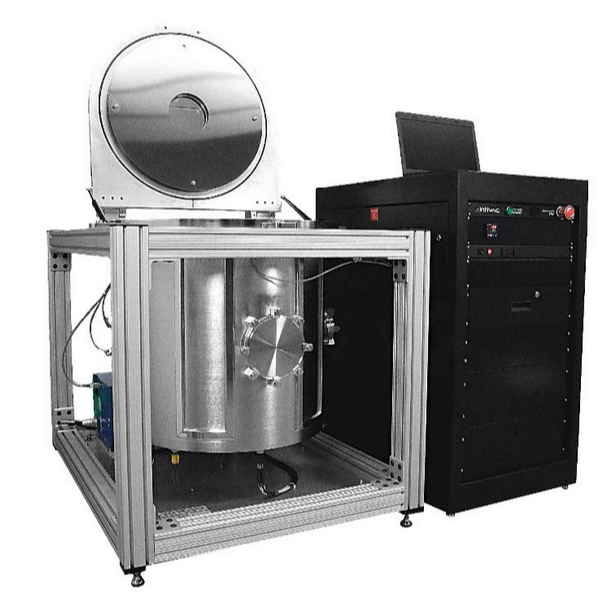
Ion Beam Sputter Deposition
Ion Beam Sputtering (IBS), also referred to as Ion Beam Sputter Deposition (IBSD), is a type of Physical Vapor Deposition (PVD) where an ion beam source is directed at a target to sputter atoms or molecules onto a substrate for deposition. IBS presents unique advantages and opens up a multitude of opportunities in industries such as optics, sensors (MEMS), thin film solar cells, and semiconductors.
High Precision Capillary Printing (HPCAP)
Effortlessly apply any material onto any surface with exceptional design flexibility using High Precision Capillary Printing (HPCAP). This innovative technique enables customised, localised manufacturing at micron and sub-micron scales without requiring masks, UV exposure, or chemical reactions.
Handling & Automation
Our selection of handling and automation equipment includes various options such as retrofit open-cassette tools, SMIF pod load/unload systems, sorters, EFEMs (Equipment Front End Modules), mass wafer and reticle transfer systems, reticle storage and handling systems, as well as robots and robotic arms.
… And more.
SiSTEM Technology excels in providing expertise and innovative solutions for the semiconductor, biotechnology, and nanotechnology R&D and manufacturing sectors. With extensive experience in the field, we take pride in assisting customers in their pursuit of advanced semiconductor tools. Our deep knowledge and guidance empower you to make informed decisions, driving innovation and success in this dynamic and evolving industry.
We offer tailored solutions across various industries including semiconductors, aerospace, batteries, medtech, and pharmaceuticals, addressing specific production requirements to enhance efficiency, precision, reliability, and quality in your manufacturing processes.
At SiSTEM Technology, we prioritise exceptional customer support as the cornerstone of our services. Through a customer-centric approach, we provide unparalleled assistance, ensuring your complete satisfaction.
Images